Our daily lives are infused with activities and interactions that rely on modern electronics enabled by nanotechnologies. Cell-phones, automotive and aviation sensors, personal and super-computers, healthcare technologies, and even our home appliances—many of which now have machine learning and artificial intelligent capabilities—are becoming ever more connected and ‘smarter”. However, with this push to deploy our devices on a global scale, our progress is increasingly being hindered by our apparent inability to further miniaturize the building block of electronics—the transistors. The transistors are already too small—of the order of 10 nanometers or so, ten thousand times smaller than a single strand of hair. In essence, we have become prisoners of fundamental physical limits of the transistor.
A potential strategy to overcome this barrier is to introduce new materials into the transistor structure to enhance their performance and functionalities. And that is the playground of Professor Asif Khan’s group of the School of Electrical and Computer Engineering at the Georgia Institute of Technology. “One of the interesting classes of functional materials that we are working on is called antiferroelectric oxides, which could lead to efficient, nanoscale logic and memory devices and devices which can even mimic the functions of biological neurons and synapses,” says Khan. In their recent work published as an Editor’s Pick in the May issue of Applied Physics Letters, they show how these mystery materials—antiferroelectrics—can be fine-tuned by doping, and how their processing techniques can be simplified to ease their entry into conventional micro- and nano-electronic fabrication technologies.
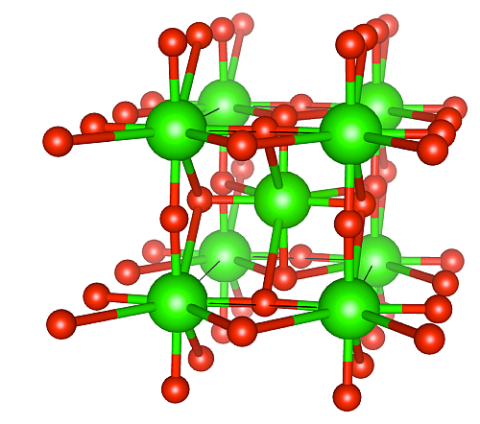
Antiferroelectric materials are electrical insulating in a way very similar to the dielectric materials used in regular capacitors. However, the significant difference is that when a certain voltage is applied across it, it undergoes a phase transition into another insulating state which is structurally different than the parent one. With appropriate nano-scale engineering, this phenomenon can be the basis for high performance logic transistors and disruptive memory technologies. Interestingly, antiferroelectricity was discovered more than 60 years ago in perovskite materials—yet it did not have a significant impact on the electronics industry despite the attractiveness because perovskites are not compatible with currently used CMOS fabrication processes. What makes the Khan group’s work particularly relevant for transistor applications is that they are studying this phenomenon in Zirconia--a very well-studied non-perovskite binary oxide which has already been in use for more than a decade in the semiconductor industry.
The major contribution of the recent work by Khan’s group is that they significantly simplified the complex process flow of stabilizing the antiferroelectric phase of zirconia. Typically, a metallic capping layer and a high temperature annealing step is required to convert dielectric zirconia into an antiferroelectric state. The group were able to eliminate these process steps through a thoughtful design process of the material stack. Khan is hopeful that this will reduce the barrier to entry of antiferroelectrics into the state-of-the-art semiconductor manufacturing processes for novel device applications. Furthermore, by introducing small amounts of lanthanum into zirconia, the researchers were able to tune the properties of antiferroelectric zirconia, namely critical field/voltage for phase transition, dielectric constant and polarization. “Such tunability can not only enable a large design space for nanoelectronic antiferroelectric devices, but also be useful for their traditional applications of antiferroelectrics in electro-calories, pyroelectrics and micro-actuators,” says Khan. He also mentions that antiferroelectricity is a close cousin of a well-known phenomenon—ferroelectricity, which being researched and adopted by major semiconductor manufacturers for potential memory applications. His previous work also focused on ferroelectric oxides for ultra-low power negative capacitance transistors. However, as he points out, antiferroelectric oxides can do all that ferroelectric oxides can but with much better endurance and reliability and reduced process complexity.
Khan’s group actively collaborated with their industry partner, Eugenus, Inc. located in San Jose, CA. “Our industry-academia partnership is vital for bringing new ideas into the fore-fronts of technology,” says Dr. Mukherjee of Eugenus, Inc., also a co-author of the paper. “We look forward to further collaboration to assess the applicability and the potential of new material and device concepts.” The Khan group also collaborated with the Charles University at Prague, Czech Republic, on structural characterization of the antiferroelectric zirconia films.
- Christa M. Ernst
“Antiferroelectricity in lanthanum doped zirconia without metallic capping layers and post-deposition/-metallization anneals” is an Editor’s Pick in May’s Applied Physics Letters. You can view the article here. https://aip.scitation.org/doi/10.1063/1.5037185
Khan’s work at Georgia Tech is supported in part by the National Science Foundation.
Additional Images
