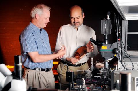
Georgia Institute of Technology researchers have developed a novel method for improving silicon-based sensors used to detect biochemicals and other molecules in liquids. The simplified approach produces micro-scale optical detection devices that cost less to make than other designs, and provide a six-fold increase in sensitivity to target molecules.
Georgia Institute of Technology researchers have developed a novel method for improving silicon-based sensors used to detect biochemicals and other molecules in liquids. The simplified approach produces micro-scale optical detection devices that cost less to make than other designs, and provide a six-fold increase in sensitivity to target molecules.
The new technique uses a thin film of porous silicon material to coat a layer of light-conducting dense silicon. The porous silicon thin film contains many connected pores and internal surfaces that greatly increase the effective area onto which a chemical component of interest – often referred to as an analyte – can bind. The increased surface area allows the porous silicon to capture larger numbers of analyte molecules, which increases overall detection sensitivity and thereby facilitates detection of analytes occurring in low concentrations.
Unlike earlier methods for generating porous silicon, the Georgia Tech thin-film process is more easily adapted for use with standard silicon-on-insulator (SOI) substrates, and also allows for highly precise control of the thickness of the porous silicon layer. The research was described in a recent paper, "Magnesiothermically Formed Porous Silicon Thin Films on Silicon-on-Insulator Optical Microresonators for High-Sensitivity Detection," published in the journal Advanced Optical Materials.
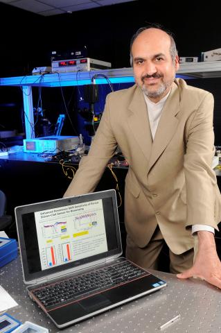
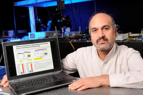
"A larger surface area means there's more room for the analytes you're seeking to land, and then to interact with the optical signal – the light – that detects them," explained Ali Adibi, Joseph M. Pettit Chair and a professor in the School of Electrical and Computer Engineering (ECE), who co-led the research along with Kenneth H. Sandhage, B. Mifflin Hood Professor in the School of Materials Science and Engineering (MSE). "And unlike other techniques, our process confines the pores to the thin film layer on top. The porous area doesn't impinge on the dense-silicon layer underneath, and consequently doesn't compromise the optical quality of the devices fabricated in the dense layer and the ability of the sensor to detect the analytes."
The work was part of the Centers in Integrated Photonics Engineering Research (CIPhER) program, a $4.3 million, two-year effort funded by the Defense Advanced Research Projects Agency (DARPA) to develop advanced laboratory-on-chip sensing technology capable of detecting multiple biological and chemical threats on a compact integrated platform. Other center participants included Emory University, Massachusetts Institute of Technology, University of California-Santa Cruz, and Yale University.
At Georgia Tech, Professor Mostafa El-Sayed of the School of Chemistry and Biochemistry and David Gottfried of the Institute for Electronics and Nanotechnology were also principal investigators on the CIPhER program. Ali A. Eftekhar, an ECE research engineer, was also part of the technical management of this project. Adibi was the lead principal investigator of this program.
Optical Detection of Analytes
The Georgia Tech researchers are working with a silicon-based optical sensor that utilizes a racetrack-shaped optical resonator capable of coupling strongly with light passing through a nearby optical waveguide at particular light frequencies. The resonator's surface is chemically functionalized to bind with specific bio-markers, chemical components or other analytes being sought.
As the optical signal passes through the silicon waveguide and resonator, the associated electromagnetic field can interact with one or more specific types of chemical components captured in the silicon surface. If an analyte is present, it alters the resonance frequency of the racetrack resonator, showing its effect on the power transmitted through the waveguide. The greater the concentration of the analyte, the larger the frequency shift, and the larger the effect on the transmitted power.
Traditionally in bio-sensing, a layer of dense silicon has served a dual purpose. It functions as the waveguide for the optical signal that detects analytes, and it also provides the surface that captures those analytes.
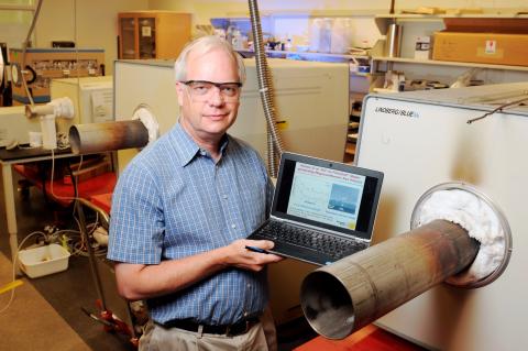
"The problem with that approach is that dense, planar silicon has limited surface area onto which analytes can bind," explained Sandhage, who is also on the faculty of the School of Chemistry and Biochemistry. "That significantly reduces how much response you get from the interaction of the light with the analyte."
Previous efforts to create pores in silicon to increase surface area have encountered drawbacks, including complexity – such as difficulty in adapting to standard silicon-on-insulator substrates – and a reduction in silicon's ability to transport optical signals, he said. One such technique, called anodization, hinges on the problematic use of a hazardous hydrofluoric acid bath with an applied electrical current to etch into doped silicon. The technique tends to yield relatively large columnar (two-dimensional) pores in doped silicon, a modest surface area, and higher loss of optical signals.
The ability to controllably convert silica into porous silicon with fine, 3-D-interconnected pores is useful in other applications besides chemical sensing, Sandhage said. These include anodes for lithium ion batteries, optical displays, and inverse opals, which are three-dimensional photonic crystals.
"The collaborative interplay between Professor Adibi's group and my group was essential to the success of this work," he said. "We both brought to bear specific techniques and expertise that enabled us to accomplish what neither of us could have done alone."
A Simpler Method
In their recent paper, the Georgia Tech teams report development of a simpler, more effective device fabrication approach. Using an oxidation process, they first grew silica (silicon dioxide) on top of the dense-silicon layer. Then, using a shape-preserving magnesiothermic reduction process, the Sandhage group exposed the silica layer to magnesium gas generated by heating magnesium silicide. The process has been patented by the Georgia Tech Research Corp. under U.S. Patent No. 7,615,206.
The resulting magnesium gas reacted with the silica layer to yield a fine mixture of silicon and magnesium oxide, but did not react with the dense-silicon layer underneath. The magnesium oxide was then easily dissolved with a weak acid solution to yield a porous silicon layer with very fine 3-D-connected pores, which trapped analytes effectively but did not appreciably scatter light and could be tailored to within about a nanometer of thickness.
Forming a reliable sensor requires careful design and optimal fabrication of the nanophotonic structures, a task that was performed in Adibi’s group. The fabrication process includes a critical step – using electron beams to cut channels in the porous silicon and underlying dense silicon, to form a patterned structure. This microlithography technique creates tiny trenches in the porous silicon and dense silicon, yielding porous-silicon-on-dense-silicon waveguides and microresonators that guide the optical signals and enable them to detect analytes.
In addition, the Adibi team used advanced computing approaches to model the materials development process and to design the sensor structures. The models helped the researchers understand which techniques were most effective for producing efficient microresonators.
"We have demonstrated that you can integrate microlithography and controlled-pore silicon on dense silicon without significantly sacrificing the quality of the resonator," Adibi said. "The result is a resonant-frequency response for sensing with much larger sensitivity – by about a factor of six – compared to when you don't have the porous silicon."
This research was supported by the Defense Advanced Research Projects Agency (DARPA). Any opinions, findings, conclusions or recommendations expressed in this article are those of the principal investigators and do not necessarily reflect the views of the sponsor, DARPA.
Research News
Georgia Institute of Technology
177 North Avenue
Atlanta, Georgia 30332-0181 USA
Media Relations Contacts: John Toon (jtoon@gatech.edu) (404-894-6986) or Brett Israel (brett.israel@comm.gatech.edu) (404-385-1933).
Writer: Rick Robinson
Additional Images
