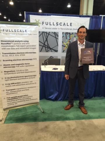
FullScaleNANO, an early-stage company that automates nanomaterial imaging and measurement and a VentureLab portfolio startup, received the TechConnect Innovation Award at the TechConnect World Innovation Conference & Expo May 22-25 in Washington, D.C.
NanoMet’s technology was developed at Georgia Tech by Chin-Hui Lee, co-founder and a professor in Georgia Tech’s School of Electrical and Computer Engineering. The company also joined VentureLab, the incubator at Georgia Tech for startups created by faculty, students, and staff. VentureLab works with those startups to help them commercialize research into viable companies.
“We created the algorithms that allow us to process thousands of images, faster and with better overall reliability,” Lee said. “This is a new frontier in science that we hope will lead to faster and more cost-effective innovation for industry.”
The company is headquartered in Tallahassee, Florida, but its software development team hub is in Atlanta.
The TechConnect Innovation Awards identify the top 15 percent of submitted technologies. Innovation rankings are based on the potential positive impact of the technology on a specific industry sector. Submissions come from global academic technology transfer offices, early-stage companies, small business innovative research awardees, and government and corporate research laboratories.
FullScaleNANO won for its NanoMet automated nanomaterials software that measures and characterizes thousands of nanomaterials in seconds.
“We are honored to receive this award that recognizes our innovative approach to measuring and characterizing nanomaterials, essential particles that are used in today’s product innovations, from medicine to manufacturing,” said Jeffrey Whalen, CEO and co-founder.
Nanomaterials are tiny particles that can’t be seen with the naked eye. The only way they can be viewed is by taking pictures with an electron microscope that contains a built-in camera. Measuring and characterizing these images is a slow, manual process — done one by one using a ruler — that takes hours, Whalen said.
NanoMet speeds up the task, using an automated system that processes images in seconds, takes thousands of measurements, and provides objective quality assurance, enabling a shorter time to market. NanoMet “sees” every individual pixel in an electron microscope image to properly identify the exact edges of nanomaterials, providing a repeatable process that saves time and money.
Nanomaterials are used or being evaluated in a variety of products from batteries to shampoos and in a number of industries from food and medicine to electronics and the environment.
In medicine alone, applications being developed for nanoparticles include delivery of chemotherapy drugs directly to cancer tumors, resetting the immune system to prevent autoimmune diseases, and delivering drugs to damaged regions of arteries to fight cardiovascular disease. Other industry uses include producing hydrogen from water, reducing the cost of producing fuel cells and solar cells, and cleaning up oil spills, water pollution, and air pollution.
Additional Images
