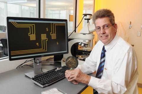
Oliver Brand is the Executive Director of the Institute for Electronics and Nanotechnology (IEN) and a professor in the School of Electrical and Computer Engineering (ECE).
Oliver Brand is the Executive Director of the Institute for Electronics and Nanotechnology (IEN) and a professor in the School of Electrical and Computer Engineering (ECE). He received his undergraduate degree in Physics from Karlsruhe Institute of Technology, Germany in 1990, and his Ph.D. degree (Doctor of Natural Sciences) from ETH Zurich, Switzerland in 1994. He was a postdoctoral fellow at Georgia Tech from 1995 to 1997 and a lecturer at ETH Zurich in Zurich, Switzerland and deputy director of its Physical Electronics Laboratory (PEL) from 1997 to 2002. In January 2003, Brand joined the Georgia Tech ECE faculty. He became the executive director of IEN in August 2013.
Why did you decide to join the ECE faculty at Georgia Tech?
The most important consideration was the microelectronics capabilities at Georgia Tech. They were world-class in two ways: one, the large number of faculty that we had in that space and two, the outstanding facilities. I’m still here 17 years later and I’ve watched our microelectronics program grow to new heights over that time, so it was a good decision.
Tell us a little about the evolution of the Institute for Electronics and Nanotechnology (IEN).
IEN is one of 12 interdisciplinary research institutes at Georgia Tech. The idea for IEN was to coalesce research in the area of electronics and nanotechnology. One way we do that is supporting research centers and labs in that area—and there is a wide variety of research that falls under our umbrella, including electronics packaging, high frequency and next-generation electronics and photonics, flexible electronics, microsensors and microactuators, energy harvesting devices, quantum sciences, micro robotics, and medical devices in partnership with Emory University, just to name a few. We have about 120 faculty involved in these centers and programs, and they come from all of the engineering disciplines, as well as the College of Sciences and the College of Computing.
The other side of what we do is managing nanotechnology core facilities. The core facilities consist of the cleanrooms in the Pettit Microelectronics Building and the Marcus Nanotechnology Building. We also have a materials characterization facility in the Marcus Nanotechnology Building that is jointly managed by IEN and the Institute for Materials.
There are more than 850 individual users from 200 faculty groups across campus using these core facilities every year. Nowadays, the core facilities annually support Georgia Tech research grants that have a total award volume around $290 million. In addition, our facilities are also used by external groups from other universities and companies, and we welcome some 150 external users. We are actually part of a national network of nanofabrication facilities, called the National Nanotechnology Coordinated Infrastructure or NNCI, which is funded by the National Science Foundation.
Why do you think Georgia Tech’s microelectronics/nanotechnology facilities have so much impact? What sets them above similar facilities around the world?
There are three main pieces. One is the Marcus Nanotechnology Building that opened in 2009. This was really thanks to James Meindl and his vision for nanotechnology research, which provided the overall infrastructure for one of the largest academic cleanrooms in the country.
The second piece is that we have world-class tools for academic research. We have a very broad toolset, which enables a wide variety of research. It’s really not just microelectronics research anymore. It’s biomedical research, materials research, energy research, and much more.
Then the third piece in the puzzle is an extraordinary staff. We couldn’t do what we do without them. We have a group of incredibly experienced research engineers, research scientists, process engineers, equipment engineers, and administrators. Many of the staff are homegrown. They did their degrees at Georgia Tech. Their high level of expertise is critical to our operations.
What do you see for the future of IEN and microelectronics research at Georgia Tech?
I think we will continue to diversify. You’ll see the tools that were traditionally used to create microelectronics devices applied to other fields as well. For instance, biomedical devices, wearable devices, advanced materials research, next generation computing, quantum sciences and technologies—I think these areas will continue to grow. I think that microelectronics and nanotechnology will continue to have a huge impact on today’s Grand Challenges.
As for our core facilities, the Marcus Nanotechnology Building has close to 10,000 square feet of unfinished cleanroom space that can be programmed depending on future needs, so there’s tremendous opportunity there. The other side, of course, is that state-of-the-art cleanroom space costs about $2,000 per square foot to build out, so that’s $20 million for the remaining unfinished space. It costs a lot of money.
My dream would be to have the funding to create an “evergreen toolset,” so that we could always bring in the newest equipment. A generous annual equipment budget would ensure that we remain competitive as one of the largest, most well-equipped facilities in the country. And, we of course need the expert staff to operate it.
