With $5.3 million in DARPA funding secured, Professor Ali Adibi is looking to light, not electricity, to move data faster and more efficiently in next-generation electronics.
(text and background only visible when logged in)

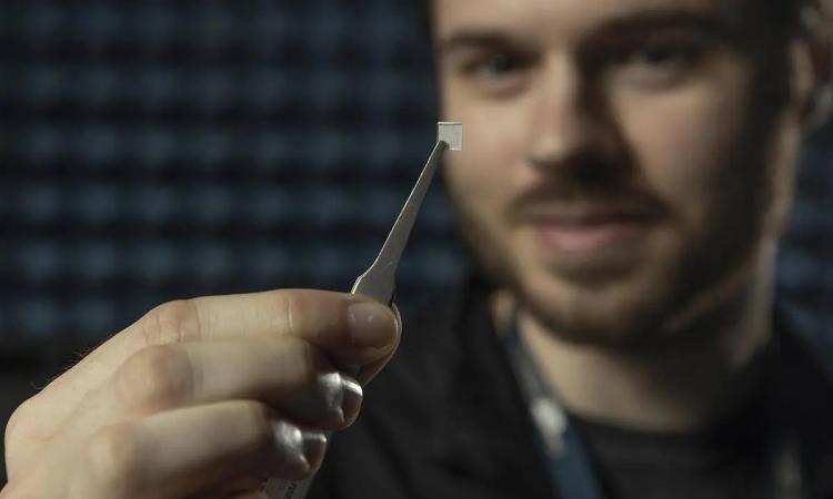
By combining advanced optical techniques, Professor Ali Adibi’s 3D optical routing system looks to enable vertical chip integration in a way not previously achieved. (Photo: Allison Carter)
(text and background only visible when logged in)
The future of computing is lit, literally.
As microchips grow more complex and data demands intensify, traditional electrical connections are hitting their limits. Speed is king in today’s digital systems, but a major bottleneck remains in how quickly information can move between components like processors and memory.
This lag is one of the most pressing challenges in advanced hardware design. While processors continue to accelerate, the links that connect them can't keep pace.
Georgia Tech researcher Ali Adibi is addressing this problem with $5.3 million in funding over three years from the Defense Advanced Research Projects Agency (DARPA). His project is part of DARPA’s Heterogeneous Adaptively Produced Photonic Interfaces (HAPPI) program, which aims to dramatically boost the speed and density of data transmission within microsystems by using light instead of electricity.
“Optical solutions are highly advantageous for providing the required data rates and power consumptions, and our project is formed to address the most important challenges for achieving the system-level performance,” said Adibi, a professor and Joseph M. Pettit Chair in the School of Electrical and Computer Engineering.
The project brings together a multidisciplinary team, including collaborators from the Massachusetts Institute of Technology, University of Florida, NY CREATES, and NHanced Semiconductors, Inc.
(text and background only visible when logged in)

A schematic illustration of a multi-chip structure with 3D optical routing. The key parts of Adibi's proposed system are: 1) multi-layer planar waveguides, 2) free-form couplers, and 3) a dense vertical waveguide array.
(text and background only visible when logged in)
Going Vertical
Unlike traditional optical communication, which connects systems across distances, this project focuses on enabling ultra-fast, low-loss communication within electronic systems.
The key innovation is vertically connecting electronic chips in a compact stack. This design helps overcome the limitations of planar optical routing geometries (layouts that guide light horizontally across a chip) which are often not compatible with the dense, 3D chip architectures needed for next-generation computing.
Adibi’s team is developing a novel 3D optical routing system that can transmit data with minimal loss, high bandwidth, and compact components. The system is designed to scale to large arrays of interconnected chips with minimal interference between data channels.
Smarter Design with Machine Learning
At the heart of the project is the use of machine learning (ML) to help design and optimize the light-based communication system.
ML is used to shape and fine-tune the tiny structures that guide light through and between chips. This includes finding the best sizes, shapes, and layouts for components like couplers and waveguides, so they can be made smaller, work more efficiently, and fit into dense chip layouts.
“Designing a complete, scalable 3D optical routing structure involves innumerable variables,” Adibi said. “Machine learning helps us navigate that complexity and find solutions that would be nearly impossible to identify manually.”
Tiny "Mirrors"
Another key innovation involves specialized optical structures, or what Adibi refers to as “artificial mirrors”.

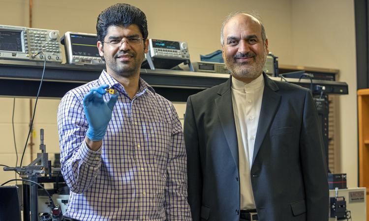
Silicon-on-insulator (SOI) wafer used in a multi-chip module featuring 3D optical interconnects. (Photo: Allison Carter)
The tiny, precisely shaped structures, called metagratings, are embedded in the chip material to redirect light vertically between layers with minimal loss. These components are designed to guide light efficiently in tight spaces, helping connect stacked chips without losing signal strength.
“Imagine light traveling through a chip and suddenly being redirected straight up. That’s the kind of precise control we’re achieving,” Adibi explained.
These innovations, along with advanced techniques for building vertical light paths through thick silicon layers and new packaging solutions that keep components precisely aligned, have shown promise on their own. But combining them is what enables dense, high-speed, low-loss communication between vertically stacked chips, something that no system has achieved before, according to Adibi.
“As with any complex system, success depends on how well everything is structured and optimized,” he said. “Once everything is in alignment, data can move faster, more efficiently, and with less energy consumption for communicating each bit of data.”
(text and background only visible when logged in)
About the Research
This research is supported by the Defense Advanced Research Projects Agency (DARPA) Heterogeneous Adaptively Produced Photonic Interfaces (HAPPI) program. Notice ID DARPA-SN-24-105.
(text and background only visible when logged in)
Related Content
New Battlefield Obscurants Could Give Warfighters Visibility Advantage
Clouds of tiny structures that are lighter than feathers could one day give U.S. warfighters and their allies the ability to observe their adversaries while reducing how well they themselves can be seen.
Shaping the Future of Light through Reconfigurable Metasurfaces
Harnessing the power of “phase-change” materials, Georgia Tech researchers have demonstrated how reconfigurable metasurfaces are crucial to the future of nanotechnology.