
A $2.2 million Semiconductor Research Corporation-supported effort brings together researchers from Georgia Tech and Purdue University to address critical challenges in advanced transistor architectures.

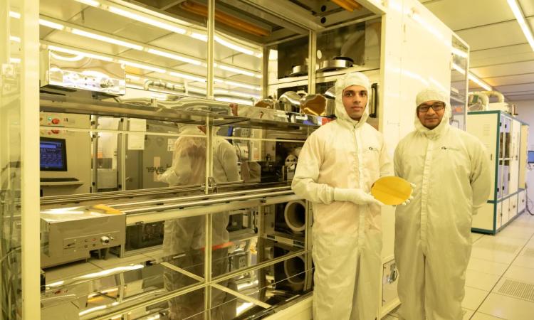
A visual representation of the project's goal to bring together data, design tools, and engineering frameworks needed to evaluate future vertically stacked transistor technologies.
The question is no longer whether researchers and industry leaders can stack transistors, but how far that approach can be pushed while maintaining performance, efficiency, and reliability.
That challenge sits at the center of the Consortium for Advanced Sequential CFET Pathfinding (CAST), a new $2.2 million Semiconductor Research Corporation (SRC)-supported effort led by Georgia Tech School of Electrical and Computer Engineering (ECE) Associate Professor Asif Khan.
“We’re at an exciting point for semiconductor research where some of the biggest advances are going to come from bringing different areas of expertise together,” Khan said. “CAST gives us an opportunity to do that around a technology that could play an important role in the future of computing.”
The effort brings together researchers from Georgia Tech and Purdue University to advance complementary field-effect transistor (CFET) technology. CFETs move transistor scaling into the vertical dimension by stacking complementary transistors on top of one another rather than positioning them side by side. That creates the potential to fit more computing capability within the same footprint, but it also introduces new questions about how the devices are built, connected, cooled, and incorporated into a chip.
The collaborative approach reflects the broader goals of SRC’s Semiconductor & Packaging Advanced Research Consortium (SPARC), which selected CAST as one of its projects. Launched in March, SPARC is designed to accelerate industry-driven university research in technologies critical to the future of the semiconductor industry.
“SPARC is built on the idea that the most important semiconductor technology challenges cannot be solved within a single technical discipline or by a single company,” said Girish Wable, technology program director at SRC.
"By bringing together leading expertise across institutions and technical domains, SPARC creates a collaborative environment where individual innovations are connected into pathfinding and system-level solutions with greater potential for industry impact, as well as creating the next generation of talent. The collaboration extends to industry members, whose input helps guide the direction of these efforts."
CAST comes as the semiconductor industry is already moving toward increasingly complex transistor architectures. Leading chipmakers are moving to gate-all-around architectures, which give greater control over the flow of current as transistors become smaller. CFETs build on many of these advances while introducing the added complexity of vertical stacking.

Khan, a leader in ferroelectric materials research, studies semiconductor materials and devices at the nanoscale as part of his work advancing next-generation transistor technologies.
“The challenge isn’t simply whether we can stack more transistors,” Khan said. “We have to understand how the devices behave, how we connect them, how we manage the heat they generate, and whether all of that ultimately translates into a better chip.”
The goal of CAST is to provide the data, design tools, and engineering frameworks needed to make those decisions.
The consortium brings together experts in four areas critical to the future of CFET development:
- Transistor and gate-stack engineering, led by Khan, focused on developing advanced materials and device technologies for vertically stacked transistors.
- Advanced contact and interconnect technologies, led by ECE Professor Suman Datta, focused on creating efficient electrical connections between devices and layers.
- Nanoscale thermal measurement and modeling, led by Purdue University Assistant Professor Raisul Islam, focused on understanding and managing heat in densely stacked architectures.
- Design-technology and system-level optimization, led by ECE Dean's Professor Shimeng Yu, focused on determining whether the benefits of multi-tier CFETs translate into meaningful improvements at the chip level.
Working together, the researchers will use artificial intelligence-driven tools to accelerate the evaluation of new materials, architectures, and manufacturing approaches.
Over the consortium's three-year effort, researchers hope to provide the semiconductor industry with the knowledge needed to evaluate and deploy future generations of stacked transistor technologies.
(text and background only visible when logged in)
Related Content
Researchers Discover New Form of NAND Flash Data Storage for Deep Space Missions
Their NAND flash memory made with ferroelectric materials can withstand extreme radiation and handle artificial intelligence applications.
(text and background only visible when logged in)
Smaller, Smarter, Speedier, Stacked: Engineering Next-Gen Computing
Some technologists suggest we’re nearing the limits of packing ever-more computing power into ever-smaller chips. At Georgia Tech, engineers are finding new ways to shrink transistors, make systems more efficient, and design better computers to power technologies not yet imagined.
(text and background only visible when logged in)